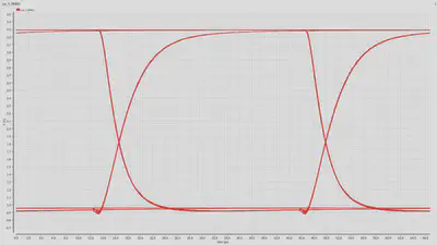
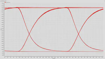
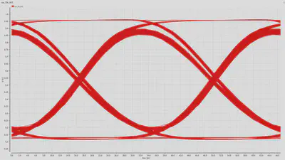
30 Gbps Silicon Photonics link
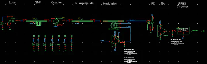
Designed 30 Gbps SiP data transmission link in Cadence Virtuoso (65 nm CMOS). The link consists of CW laser, CMOS driver, MRM, PD, and TIA. SiP devices are modelled in Verilog-A. The driver has cascode common-source topology whereas the TIA is based on 3-stage inverters. Energy efficiency of 1.98 pJ/bit was achieved.


Dias Azhigulov
Master student in Electrical and Computer Engineering
I find joy in learning about computers & related technologies both on software and hardware level.