Sub-Sampling LC-PLL design
Introduction
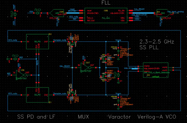
Sub-Sampling Phase-Locked Loops (SS PLLs) offer several advantages over classical Phase-Frequency Detector Charge Pump (PFD-CP) based PLLs such as lower phase noise (PN), higher loop bandwidth (BW), and reduced power consumption due to its simplicity. Inspired by the findings reported in the original paper, we attempt to recreate the results by building the same circuit. All the devices are implemented using TSMC 65 nm PDK components.
Before diving into circuit details, it should be emphasized that we use Verilog-A VCO model and tune its parameters to suit our needs:
| Parameter | Value |
|---|---|
| VCO gain | 90 MHz/V |
| VCO bank gap | 20 MHz |
| VCO frequency | 2.6 GHz |
| FLL division | 24 |
Sub-sampling Phase Detector and Loop Filter
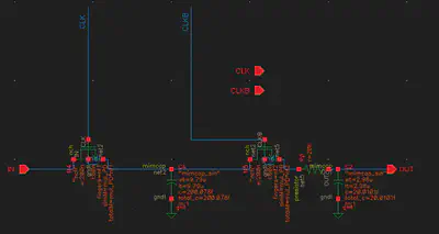
Fig. 1 depicts our SS PD circuit diagram. Note that this circuits acts both as SS PD and Loop Filter (LF) because two transistors and a capacitor can effectively be seen as a series resistance R1, which is defined by: $$ R_1 = \frac{1}{f_{ref}*C_1} $$ Another important observation is that contrary to what is proposed in the reference paper, we omitted the stabilizing zero path since phase margin is not of concern due to the presence of Verilog-A Voltage- Controlled Oscillator (VCO). We also do not place any dummy transistors as charge sharing effect is not captured in the simulation. Thus, we have two transistor whose $\frac{W}{L} = \frac{2000}{60}$. We keep the resistor R2 value to be the same as in the original paper (20kΩ), however, C1 and C2 should be carefully selected. The reason has to do with the fact that this SS PD can be viewed as an RC circuit with BW of: $$ BW_{PD+LF} = \frac{1}{2\pi(R_1+R_2)C_2}=\frac{1}{2\pi(\frac{C_2}{f_{ref}C_1}+R_2C_2)} $$ which attenuates the incoming signal proportional to $\frac{C_2}{C_1}$. Therefore, one has to increase $C_1$ while keeping $C_2$ at minimum. However, this comes at a cost of the area and clock feedthrough, which could be filtered out by using larger $C_2$. Having this intuition, we decided to set $C_2 = 20 fF$ and $C_1 = 200 fF$, which adequately suppresses clock feedthrough while keeping the control voltage between $\sim\pm200 mV$.
Synthesized Frequency-Locked Loop
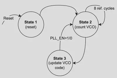
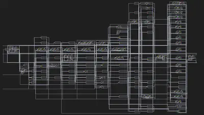
Another important block in the proposed SS PLL is FLL. Our FLL is implemented digitally using Verilog. The code is provided in the Appendix section. To develop the code we started with the FSM diagram demonstrated in Fig. 3, which is a simplified version of the original FSM, where the authors have an extra state for power savings. In contrast, our code, regardless of the outcome of State 3 (i.e. PLL_EN = 1/0), returns to State 2 and starts counting again. When the reset is enabled, the capacitor bank is initialized to a 32-bit word that sets VCO to 2.4 GHz. There are two always blocks in the Verilog code, one for counting the VCO cycles and another for state transition and output logic. The latter is synchronized to the reference clock to minimize random jitter effects on the FLL output. Afterwards, the code is sourced into Cadence Genus for Register Transfer Level (RTL) synthesis. The result is shown in Fig. 4.
The division ratio is supplied as an 8-bit input to FLL, which then outputs 32-bit capacitor bank code word and sets CAL_READY (PLL_EN in the Verilog code) node to 1 or 0 in Fig. 2. This signal, in its turn, connects Vcontrol to SS PD and if disconnected, sets it to 0V differential using an inverter and a pair of NMOS transistors (all min. width). It should be mentioned that the ADC and DAC in Fig. 2 are behavioural models that are used to facilitate visualization of digital bus signals.
System-level Simulations
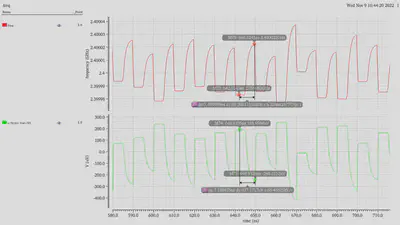
Once all the blocks are designed and tuned for target specifications, the PLL is simulated for various scenarios including target frequency change, phase step in reference clock, and noise analysis. Fig. 5 illustrates the behaviour of the PLL for various target frequencies. It can be deduced that the proposed PLL successfully locks for all conditions with a good settling time. Although we designed our FLL and configured VCO in such a way as to have 2.3, 2.4, and 2.5 GHz frequencies at the middle of the tuning curves, which ideally correspond to $V_{control}$ = 0V , there are cases when FLL lets PLL to takeover the control one frequency step before its expected value. Consequently, in order to lock PLL increases $V_{control}$ up to 200 mV to compensate for this small error in FLL. This is only observed when moving down the tuning curves, regardless of the target frequency. When moving up the curves, the FLL behaves as expected, therefore PLL keeps $V_{control}$ at around 0V. This problem was further investigated by visualizing the nodes inside FLL and it seems that the issue originates from the irregularities in the phase of VCO. As a consequence, the FLL counts 1 less VCO cycle and thinks that it is at the correct frequency. It is for this reason that when target frequency is increased, the first step is twice as big as any other subsequent frequency step (40 MHz jump instead of 20 MHz).
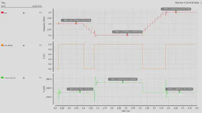
Settling time is estimated to be 670 ns for 100 MHz frequency steps and it take 1.1 $\mu s$ to move 200 MHz.
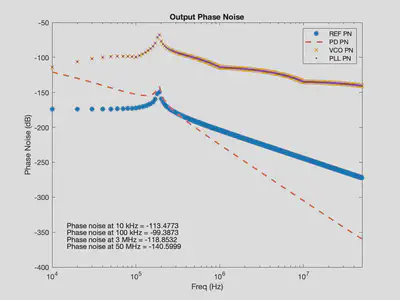
The above figure illustrate the phase noise performance of our SS PD and the entire PLL. We simulate the phase noise of SS PD in Cadence and import the result into MATLAB code where the system level phase noise analysis is conducted based on available VCO and reference clock data. Additionally, we provide in-band and out-of-band phase noise values in the figure above.
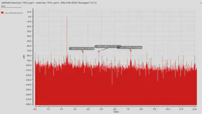
According to the plot above, it can be seen that the largest spur is around -70.3 dB.
Furthermore, we visualize the impact of clock feedthrough on VCO output frequency and control line. The oscillation magnitude was calculated to be less than 1000 ppm (approx. 40 kHz), thereby satisfying the specification.
Conclusion
To sum up, in this report we demonstrated the block and transistor level diagram of the proposed SS PLL. We provided reasoning behind some design choices for SS PD and explained the Verilog code used to synthesize the FLL. In the results section we discussed the system level simulation results and provided explanation to some of the phenomena observed in figures. While these figures are not be the best, they still meet all the specifications.
Dias Azhigulov
Master student in Electrical and Computer Engineering
I find joy in learning about computers & related technologies both on software and hardware level.