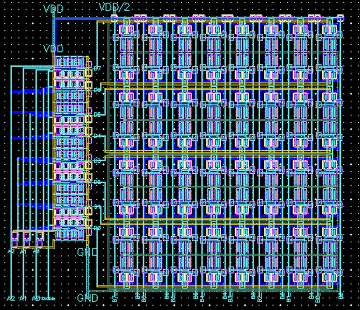
6T SRAM memory cell design and layout
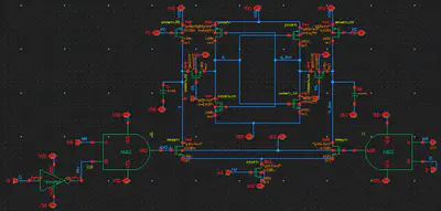
Implementation of SRAM circuit with write drivers. The circuit can discharge the bit line at 100 mV per 297 ps. This circuit also meets write operations requirements as the pass gate is able to pull the internal node (q_bar) well below $\frac{V_s}{2}$, which was found to be 0.278V. Q_bar is completely pulled down to 0 and q is pulled up to the maximum value of 1.
Dias Azhigulov
Staff Analog Design Engineer
I find joy in learning about computers & related technologies both on software and hardware level.