Two-Stage OTA design using gm/Id methodology
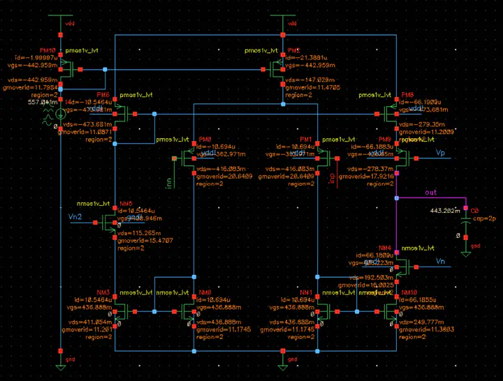
Designed two-stage OTA in 45 nm CMOS using gm/Id sizing for target specs. Achieved 52 dB gain, 187 MHz UGBW, 7 ns settling time, 800 mV output swing while consuming 99 μW power.
Dias Azhigulov
Master student in Electrical and Computer Engineering
I find joy in learning about computers & related technologies both on software and hardware level.